Low pressure chemical vapor deposition (LPCVD) is a deposition technology that uses heat to initiate a reaction of a precursor gas on the solid substrate. This reaction at the surface forms the solid phase material. Low pressure (LP) is used to decrease any unwanted gas phase reactions, and also increases the uniformity across the substrate.
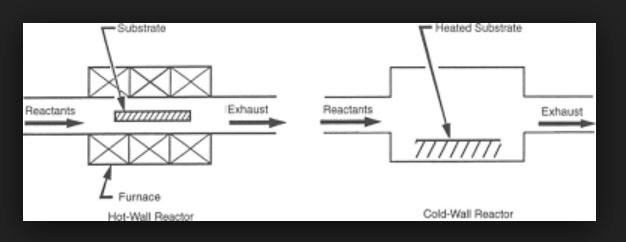
The LPCVD process can be done in a cold or hot walled quartz tube reactor. Hot walled furnaces allow batch processing and therefore gives high output. They also provide good thermal uniformity which result in uniform film deposition. A disadvantage of hot wall systems is that deposition also occurs on the furnace walls. This requires more maintenance and cleaning. Some times we need to replace the tube to avoid falling of flakes of deposited material which can contaminate the process.
Cold wall reactors are lower maintenance as there is no film deposition on the reactor walls.
In LPCVD, the tube is evacuated to low pressures from 10m Torr to 1 Torr. Once the tube is under vacuum, the tube is then heated up to deposition temperature, which is similar to the decomposing temperature of the precursor gases.
The temperatures can range from 425-900°C depending on the process and the reactive gases being used. Gas is injected into the tube, where it diffuses and reacts with the surface of the substrate creating the solid phase material. Any excess gas is then pumped out of the tube and goes through an exhaust treatment system.
LPCVD films are typically more uniform, lower in defects, and exhibit better step coverage than films produced by PECVD and PVD techniques.
The disadvantage of LPCVD is that it requires higher temperatures, which puts limitations on the types of substrate and materials used.
Materials deposited
Poly-silicon, silicon nitride, silicon oxynitride, and silicon dioxide can be deposited using LPCVD.
Poly-silicon can be deposited as both undoped and P or N doped.
Common uses of polysilicon are wire traces for both IC and MEM’s devices, including neural (brain) probes. Sacrificial layers in pressure sensors and other MEM’s devices.
It is also commonly used as a structural layer in surface micro machine devices. It can also be used in radiation detectors.
After deposition the poly-silicon can be annealed to fine tune the stress.
Silicon nitride can be deposited in both stoichiometric (stoichiometry is using balanced chemical equation to calculate amounts of reactants and products.) form (Si3N4) and low-stress (silicon-rich) form depending on the material properties needed.
Low-stress nitride is good for making membranes that are also resistant to HF etching.
Stoichiometric silicon nitride is used as an insulator, dielectric, and chemical and/or water barrier in MEMS devices, neural probes, and IC’s.
Silicon oxide can be deposited in three different ways and each method has different properties.
High temperature oxide (HTO) is deposited at around 900°C and is somewhat conformal, making it suitable for sidewall coating and some trench refill applications as long as the aspect ratio is not too severe.
HTO is the highest quality LPCVD oxide making it suitable for applications where a high-quality dielectric is required.
The best quality oxide is a thermally grown film rather than LPCVD.
Oxide can also be deposited by the hydrolysis of TEOS (tetraethyl orthosilicate) into silicon dioxide.
Silicon dioxide formed by this reaction is the most conformal LPCVD process and can be excellent for trench refill and coating higher aspect ratio features or through wafer vials that require electrical isolation.
TEOS material properties similar to that of LTO but can be adjusted after annealing in steam to be similar to those of thermal oxide. At the low temperature end of the scale at 400°C is Low Temperature Oxide Low temperature oxide (LTO) which is the lowest quality LPCVD oxide which also has less conformality and less gap fill capability.
Products manufactured using LPCVD
- Thin film Transistors
- Thin film photovoltaic solar cells
- Resistors
- Capacitor dielectrics
- MEMS
- Passivation
- Anti-reflection layers
- Trench refill
For More articles on Vacuum Technology please subscribe
Pingback: Chemical vapour deposition